
Search


OSP Surface Treatment for FPC: Characteristics, Design Production Notes, Application Fields
- Dec 25,2025
-
Share
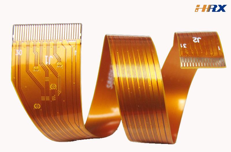
In the field of Flexible Printed Circuit (FPC) manufacturing, surface treatment technology is a crucial link that directly affects the solderability, reliability, and service life of FPC products. Among various surface treatment processes, Organic Solderability Preservatives (OSP) has been widely concerned and applied by FPC manufacturers due to its unique advantages. As a global ODM/OEM manufacturer in the field of FPC, PCB and rigid-flex boards, Shenzhen Huaruixin Electronics Co., Ltd. has rich production experience in OSP surface treatment technology. This article will deeply analyze the characteristics of OSP surface treatment, key details that need attention in the design and production process, effective methods to avoid related problems, and its wide application fields, aiming to provide professional reference for peers in the industry.
1. Core Characteristics of OSP Surface Treatment for FPC
OSP, also known as organic solderability preservative, is a surface treatment process that forms a thin organic film on the surface of the copper foil of FPC to protect the copper surface from oxidation and ensure good solderability during the soldering process. Combined with the practical production experience of Shenzhen Huaruixin Electronics Co., Ltd., the core characteristics of OSP surface treatment are mainly reflected in the following aspects:
1.1 Simple Process and Easy Process Control
The general process of OSP surface treatment for FPC includes degreasing → micro-etching → acid cleaning → pure water cleaning → organic coating → cleaning. Compared with other surface treatment processes such as Electroless Nickel Immersion Gold (ENIG), Hot Air Solder Leveling (HASL), and Immersion Silver (ImAg), the OSP process flow is simpler, and each process link is easy to control. During the production process, FPC manufacturers can realize continuous and stable production through standardized operation procedures, which effectively reduces the difficulty of process control and the probability of defective products. Shenzhen Huaruixin Electronics Co., Ltd. has optimized the OSP process parameters according to the characteristics of different FPC products, further improving the stability and consistency of the process.
1.2 Flat Surface and Suitable for SMT and Lead-Free Soldering
One of the most prominent advantages of OSP surface treatment is that it can form a very flat surface on the FPC copper surface. This flat surface is crucial for Surface Mount Technology (SMT), as it ensures good contact between the solder paste and the copper pad, improving the soldering accuracy and reliability. At the same time, OSP film is compatible with lead-free soldering requirements. With the increasingly strict environmental protection requirements in the global electronics industry, lead-free soldering has become a mainstream trend, and OSP surface treatment can well meet this development demand. In addition, the flat surface of OSP also helps to reduce the occurrence of soldering defects such as bridging and insufficient soldering during the SMT process.
1.3 Convenient Rework and Horizontal Line Operation
OSP surface treatment has good rework performance. If there is a problem in the soldering process, the OSP film on the FPC surface can be removed through appropriate methods, and then the OSP treatment and soldering can be performed again, which effectively reduces the loss caused by production errors. Moreover, the OSP process is suitable for horizontal line operation, which can realize continuous production of FPC, improve production efficiency, and reduce production costs. Shenzhen Huaruixin Electronics Co., Ltd. has introduced advanced horizontal OSP production lines, which can meet the mass production needs of different specifications of FPC products.
1.4 Compatibility with Multiple Treatments and Low Cost
OSP surface treatment has good compatibility, and can coexist with other surface treatment processes on the same FPC board, such as OSP + ENIG. This characteristic makes OSP very flexible in the production of FPC products with complex requirements, and can meet the different soldering and reliability requirements of different areas of the board. In addition, compared with processes such as ENIG, the raw materials and production costs of OSP are lower, which can help FPC manufacturers reduce production costs under the premise of ensuring product quality. At the same time, the OSP process does not produce harmful substances such as heavy metals, which is more environmentally friendly and meets the global environmental protection development requirements.
1.5 Certain Limitations
While OSP has many advantages, it also has certain limitations. First, there is a limit to the number of reflow soldering times. The OSP film will be gradually damaged with the increase of reflow soldering times. Generally speaking, 2 times of reflow soldering can be guaranteed without affecting the soldering performance, but more than 2 times may lead to the failure of the OSP film. Second, it is not suitable for crimping technology and wire bonding. The OSP film is relatively thin and has poor wear resistance, which cannot meet the requirements of crimping and wire bonding for surface hardness and wear resistance. Third, visual inspection and electrical testing are inconvenient. The OSP film is transparent, which makes it difficult for operators to visually inspect the quality of the surface treatment, and also brings certain difficulties to electrical testing. Fourth, N2 gas protection is required during SMT. In order to prevent the oxidation of the OSP film during high-temperature reflow soldering, N2 gas protection must be used to ensure the soldering effect. Fifth, it is not suitable for SMT rework. The high temperature during rework will further damage the OSP film, affecting the re-soldering performance. Sixth, the storage conditions are relatively strict. OSP-treated FPC products need to be stored in a dry, low-humidity environment to avoid oxidation of the copper surface due to moisture.
2. Key Details to Pay Attention to in OSP Surface Treatment Design and Production of FPC
In order to give full play to the advantages of OSP surface treatment and avoid quality problems, Shenzhen Huaruixin Electronics Co., Ltd. summarizes a series of key details that need attention in the design and production process based on years of production experience. These details run through the entire process from product design to mass production.
2.1 Product Design Stage
2.1.1 Rational Design of Pad Size and Spacing
In the design stage of FPC products using OSP surface treatment, the size and spacing of the pads must be reasonably designed. Due to the good flatness of OSP, it is suitable for small-pitch SMT components, but the pad size should not be too small, otherwise it will affect the adhesion of the OSP film and the soldering reliability. Generally speaking, the minimum pad size should be matched with the size of the SMT components, and the pad spacing should be greater than the minimum process requirement to avoid bridging during soldering. Shenzhen Huaruixin Electronics Co., Ltd. will provide professional design suggestions according to the customer's product requirements, ensuring that the pad design meets the OSP process requirements and the soldering requirements of the components.
2.1.2 Confirmation of Surface Treatment Area
If the FPC product needs to use multiple surface treatment processes such as OSP + ENIG, it is necessary to clearly define the surface treatment area of each part in the design stage. The boundary between different treatment areas should be clear, and there should be no overlapping or missing areas. This requires accurate positioning in the design drawing and clear marks. Shenzhen Huaruixin Electronics Co., Ltd. will use advanced CAD design software to assist customers in optimizing the design of the surface treatment area, ensuring the accuracy and rationality of the process implementation.
2.1.3 Consideration of Storage and Transportation Conditions
Since OSP-treated FPC products have strict requirements on storage conditions, the design of the product's packaging and transportation method should be considered in the design stage. It is recommended to use moisture-proof packaging materials, and add desiccants in the packaging to ensure that the product is in a dry environment during storage and transportation. At the same time, the transportation process should avoid violent collision and extrusion to prevent damage to the OSP film. Shenzhen Huaruixin Electronics Co., Ltd. will customize the appropriate packaging scheme according to the characteristics of the product and the transportation distance.
2.2 Production Process Stage
2.2.1 Control of Degreasing Process
Degreasing is the first step of the OSP process, and its main purpose is to remove oil stains, dust and other impurities on the surface of the FPC copper foil. The quality of degreasing directly affects the adhesion of the subsequent OSP film. During the degreasing process, it is necessary to strictly control the concentration of the degreasing agent, the temperature and the treatment time. If the degreasing is not sufficient, the OSP film will have poor adhesion and easily fall off; if the degreasing is excessive, it will corrode the copper surface and affect the soldering performance. Shenzhen Huaruixin Electronics Co., Ltd. uses automatic degreasing equipment, which can real-time monitor and adjust the degreasing parameters to ensure the degreasing effect.
2.2.2 Control of Micro-Etching Process
Micro-etching is to form a uniform rough surface on the copper foil surface through chemical etching, which can improve the adhesion between the OSP film and the copper surface. The key parameters of the micro-etching process include the concentration of the micro-etching solution, the temperature and the etching time. The etching depth should be controlled within a reasonable range, generally 0.3-0.5 μm. If the etching depth is too shallow, the adhesion of the OSP film is not enough; if the etching depth is too deep, it will reduce the thickness of the copper foil and affect the electrical performance of the FPC. Shenzhen Huaruixin Electronics Co., Ltd. regularly detects the concentration and etching rate of the micro-etching solution to ensure the stability of the micro-etching effect.
2.2.3 Control of Acid Cleaning and Pure Water Cleaning Process
After micro-etching, acid cleaning is required to remove the copper ions and other impurities remaining on the copper surface. The acid cleaning solution generally uses dilute sulfuric acid or hydrochloric acid, and the concentration and treatment time should be strictly controlled to avoid excessive corrosion of the copper surface. After acid cleaning, pure water cleaning must be performed thoroughly to remove the acid solution and impurities on the surface. The purity of pure water should meet the requirements of 18MΩ·cm, and the number of cleaning times should not be less than 3 times to ensure that there is no residual acid solution on the surface. Shenzhen Huaruixin Electronics Co., Ltd. uses multi-stage pure water cleaning equipment, which can ensure the cleaning effect and avoid the impact of residual impurities on the subsequent OSP coating.
2.2.4 Control of Organic Coating Process
Organic coating is the core link of the OSP process, and the quality of the coating directly determines the performance of the OSP film. During the coating process, it is necessary to control the concentration of the OSP solution, the temperature, the coating time and the withdrawal speed. The thickness of the OSP film should be controlled between 0.2-0.5 μm. If the film thickness is too thin, it cannot effectively protect the copper surface; if the film thickness is too thick, it will affect the soldering performance. Shenzhen Huaruixin Electronics Co., Ltd. uses automatic coating equipment, which can accurately control the coating parameters and ensure the uniformity and consistency of the OSP film thickness.
2.2.5 Control of Post-Coating Cleaning and Drying Process
After organic coating, it is necessary to clean the surface of the FPC to remove the excess OSP solution on the surface. Then, drying treatment is performed to remove the moisture on the surface and ensure the adhesion of the OSP film. The drying temperature should be controlled between 80-120℃, and the drying time should be 5-10 minutes. If the drying is not sufficient, the OSP film will easily absorb moisture and cause oxidation of the copper surface. Shenzhen Huaruixin Electronics Co., Ltd. uses hot air circulation drying equipment, which can ensure uniform drying of the product and avoid local moisture residue.
2.3 Quality Inspection Stage
Quality inspection is an important guarantee for the quality of OSP surface treatment. The inspection items mainly include the appearance of the OSP film, film thickness, adhesion, solderability and so on. For the appearance inspection, it is necessary to check whether the OSP film is uniform, transparent, and free of defects such as bubbles, wrinkles, and peeling. The film thickness can be measured using a film thickness gauge. The adhesion test can be performed by the tape test method. The solderability test can be performed by the reflow soldering test. Shenzhen Huaruixin Electronics Co., Ltd. has established a complete quality inspection system, and each batch of OSP-treated FPC products must pass strict inspection before leaving the factory to ensure product quality.
3. Methods to Avoid Problems in OSP Surface Treatment of FPC
In the actual production process of OSP surface treatment of FPC, various problems may occur due to factors such as process parameters, raw materials, and equipment. Shenzhen Huaruixin Electronics Co., Ltd. summarizes the common problems and corresponding avoidance methods based on practical experience, which can effectively improve the qualified rate of products.
3.1 Problem of Poor Adhesion of OSP Film
3.1.1 Causes
The main causes of poor adhesion of the OSP film include insufficient degreasing, incomplete micro-etching, residual impurities on the copper surface, and inappropriate OSP solution parameters.
3.1.2 Avoidance Methods
First, strictly control the degreasing process parameters to ensure that the oil stains and impurities on the copper surface are completely removed. Second, optimize the micro-etching parameters to ensure that the copper surface forms a uniform rough surface. Third, strengthen the pure water cleaning process to ensure that there is no residual acid solution and impurities on the copper surface. Fourth, regularly detect and adjust the concentration, temperature and other parameters of the OSP solution to ensure that it meets the process requirements. In addition, the FPC substrate should be inspected before production to avoid using substrates with contaminated surfaces.
3.2 Problem of Oxidation of Copper Surface
3.2.1 Causes
The oxidation of the copper surface after OSP treatment is mainly caused by insufficient film thickness of the OSP film, poor drying effect, improper storage conditions, and excessive reflow soldering times.
3.2.2 Avoidance Methods
First, accurately control the OSP coating parameters to ensure that the film thickness meets the requirements. Second, strengthen the drying process to ensure that the product is completely dry. Third, strictly control the storage conditions, store the product in a dry, low-humidity environment, and use moisture-proof packaging. Fourth, limit the number of reflow soldering times, and try to control it within 2 times. If multiple soldering is required, appropriate process measures can be taken, such as using N2 gas protection to reduce the oxidation of the OSP film.
3.3 Problem of Poor Soldering Performance
3.3.1 Causes
Poor soldering performance is mainly caused by excessive thickness of the OSP film, oxidation of the OSP film, contamination of the pad surface, and inappropriate soldering parameters.
3.3.2 Avoidance Methods
First, strictly control the thickness of the OSP film to ensure that it is within the range of 0.2-0.5 μm. Second, avoid oxidation of the OSP film by controlling the number of reflow soldering times and using N2 gas protection. Third, ensure that the pad surface is clean and free of contamination before soldering. Fourth, optimize the soldering parameters, such as soldering temperature, time and speed, to ensure that the OSP film can be completely decomposed during soldering and the copper surface can fully contact the solder paste. Shenzhen Huaruixin Electronics Co., Ltd. will conduct soldering tests on each batch of products to ensure that the soldering performance meets the requirements.
3.4 Problem of Inconvenient Visual Inspection and Electrical Testing
3.4.1 Causes
Due to the transparency of the OSP film, it is difficult to observe the surface quality with the naked eye, and the electrical conductivity of the OSP film is poor, which affects the electrical testing effect.
3.4.2 Avoidance Methods
For visual inspection, special detection equipment such as a microscope can be used to observe the surface of the OSP film to check for defects such as bubbles, wrinkles, and peeling. For electrical testing, appropriate testing methods and equipment can be selected, such as using a four-probe tester to test the conductivity of the pad, or using a test fixture to ensure good contact between the test probe and the pad. In addition, marking can be made on the non-functional area of the FPC during the design stage to assist in the positioning and inspection of the test.
4. Application Fields of FPC Products with OSP Surface Treatment
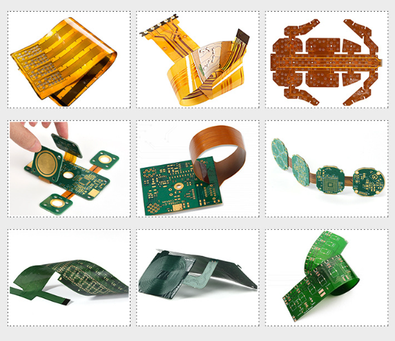
Due to its advantages of flat surface, good solderability, low cost and environmental friendliness, OSP surface treatment is widely used in various fields that require FPC products. Shenzhen Huaruixin Electronics Co., Ltd. has provided OSP-treated FPC products for many customers in different fields, and has accumulated rich application experience. The main application fields are as follows:
4.1 Consumer Electronics Field
The consumer electronics field is the largest application market for FPC products, and OSP surface treatment is widely used in products such as mobile phones, tablets, laptops, digital cameras, and wearable devices. These products have the characteristics of small size, light weight, and high integration, requiring FPC products to have good SMT compatibility and soldering reliability. The flat surface of OSP surface treatment can meet the requirements of small-pitch SMT components, and the low cost can help reduce the production cost of consumer electronics products. For example, in mobile phone motherboards and camera modules, OSP-treated FPC products are widely used to connect various components such as chips, sensors, and displays.
4.2 Automotive Electronics Field
With the development of the automotive electronics industry, the demand for FPC products in automotive electronic systems is increasing. OSP surface treatment is suitable for automotive electronic products such as automotive infotainment systems, automotive navigation systems, automotive sensors, and automotive lighting systems. These products require good reliability and stability under harsh working environments such as high temperature, high humidity, and vibration. The OSP film can effectively protect the copper surface from oxidation, ensuring the long-term stable operation of the FPC product. Shenzhen Huaruixin Electronics Co., Ltd. has passed the automotive industry quality certification, and its OSP-treated FPC products can meet the strict quality requirements of the automotive electronics field.
4.3 Medical Device Field
Medical devices have high requirements for product quality and reliability, and FPC products used in medical devices need to have good biocompatibility, soldering reliability and long-term stability. OSP surface treatment is widely used in medical devices such as medical monitors, medical scanners, and implantable medical devices. The environmental friendliness of OSP process ensures that there is no heavy metal pollution in the product, which meets the biocompatibility requirements of medical devices. At the same time, the good soldering performance of OSP ensures the reliable connection of various components in the medical device, ensuring the normal operation of the device.
4.4 Industrial Control Field
In the industrial control field, FPC products are used in industrial control systems, industrial sensors, industrial robots and other equipment. These products need to work stably in harsh industrial environments, requiring FPC products to have good anti-interference performance, soldering reliability and durability. OSP surface treatment can meet these requirements, and its low cost and convenient production make it widely used in the industrial control field. For example, in industrial robot joints and sensors, OSP-treated FPC products are used to realize signal transmission and control.
4.5 Other Fields
In addition to the above fields, OSP surface treatment is also used in aerospace, military electronics and other fields. These fields have extremely high requirements for the reliability and stability of FPC products, and OSP surface treatment can meet the relevant requirements through strict process control and quality inspection. Shenzhen Huaruixin Electronics Co., Ltd. can customize OSP-treated FPC products according to the special requirements of different fields to meet the diverse needs of customers.
5. Conclusion
OSP surface treatment is an important surface treatment process in FPC manufacturing, with the advantages of simple process, flat surface, good solderability, low cost and environmental friendliness. However, it also has certain limitations, such as the limit of reflow soldering times and strict storage conditions. In the design and production process of OSP surface treatment, it is necessary to pay attention to key details such as pad design, process parameter control, and quality inspection, and take effective measures to avoid problems such as poor adhesion of OSP film, oxidation of copper surface, and poor soldering performance.
As a global ODM/OEM manufacturer in the field of FPC, PCB and rigid-flex boards, Shenzhen Huaruixin Electronics Co., Ltd. has rich experience in OSP surface treatment technology and can provide customers with high-quality OSP-treated FPC products. If you have related project needs, we are a professional manufacturer and welcome you to contact us at any time. For more industry knowledge, you can also visit our website: www.hrxfpc.com or email us at sales@hrxfpc.com for consultation, to exchange and learn together and get guidance.

Let’s talk! We’ll provide the perfect solution for you!
-
 Huaruixin Electronics mainly produces printed circuit boards as the core business, to provide customers with one-stop solutions for FPC/PCB production, components sourcing and Assembly.
 - WHAT WE DO — PCB Design Solutions — Flex PCB Production — Components Sourcing — FPC&PCB Assembly
- PRODUCTS — Single Sided Flexible Circuits — Double Sided Flexible Circuits — Multilayer Flexible Cirucits — Rigid-Flex Circuits — FPC Assembly — PCB Assembly
- CAPABILITY — FPC Capability — Rigid-Flex Capability — PCB Capability — Assembly Capability
- Copyright © 2024 Shenzhen Huaruixin Electronics Co., Ltd. All Rights Reserved.
- Design By BONTOP