
Search


Do White/Gray Spots on Film Layers Jeopardize Product Quality? Key Handling Insights
- Oct 07,2025
-
Share
In the manufacturing of Flexible Printed Circuits (FPC), Printed Circuit Boards (PCB), and rigid-flex boards, film layers (such as solder masks and coverlays) act as critical protective and functional barriers. A prevalent question in the industry is: Do white/gray spots on these film layers undermine product quality? The answer is unequivocally yes. These spots are far from mere cosmetic blemishes; they signal underlying issues that can erode core product performance:
They may diminish insulation resistance, increasing the risk of electrical leakage in precision electronic devices.
They can weaken the adhesion between film layers and substrates, triggering delamination—a fatal flaw for products used in vibration-prone environments like automotive or aerospace applications.
In severe cases, they disrupt electrical signal transmission, leading to malfunctions in sensitive equipment such as medical monitors or industrial control systems.
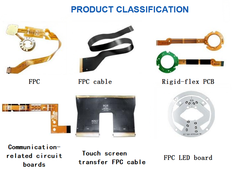
As a global-leading ODM/OEM manufacturer specializing in FPC, PCB, and rigid-flex boards, Shenzhen Huaruixin Electronics Co., Ltd. is well-equipped to address film layer defects. Boasting large-scale production bases, cutting-edge R&D capabilities, and certifications including GB/T19001-2016/ISO 9001:2015 Quality
Management System, IAF International Accreditation, and CNAS National Accreditation, we guarantee product stability and reliability through systematic quality control. Below, we detail the key considerations for addressing white/gray spots on film layers, organized by priority to facilitate effective problem-solving:

1. Core Priority: Root Cause Analysis (The Cornerstone of Effective Resolution)
Without identifying the root cause, any corrective action is merely a temporary fix. Focus on three critical areas during investigation:
Workshop Environment: Monitor humidity and particulate levels. Humidity exceeding 60% RH can trap moisture between the film and substrate, which solidifies into white spots after curing. Dust particles (larger than 5μm) often create voids that manifest as gray spots.
Raw Material Integrity: Inspect film materials (solder mask ink, coverlay) for quality and storage compliance. Expired materials, contaminated batches, or storage in environments with direct sunlight/moisture degrade film composition, leading to spot formation.
Process Parameter Accuracy: Review lamination and curing parameters. Insufficient lamination pressure (below 0.3MPa) leaves air bubbles (appearing as gray spots); uneven curing temperature (variations >±5℃) or incomplete curing time (less than 80% of the recommended duration) results in incomplete resin cross-linking, causing white hazy areas.
2. Essential Step: Precision Detection & Verification (Avoid Misjudgment of Defects)
Accurate defect assessment prevents overcorrection (wasting resources) or undercorrection (compromising quality). Adopt industry-standard testing methods:
High-Resolution Microscopy: Use optical microscopes (magnification ≥50x) or scanning electron microscopes (SEM) to analyze spot morphology—distinguishing between voids, impurities, or resin defects—and measure their size and depth.
Adhesion Strength Testing: Conduct peel strength tests in accordance with IPC-TM-650 2.4.9. A peel strength drop of more than 20% compared to standard values indicates potential delamination risks.
Insulation Resistance Measurement: Use a megohmmeter to test insulation resistance between the film layer and substrate. Values below 10^10 Ω·cm confirm that spots have impaired electrical insulation.
3. Critical Action: Targeted Defect Handling (Balance Quality & Cost-Efficiency)
Classify defects by severity and implement corresponding measures:
Severe Defects: Spots larger than 0.5mm, or those causing insulation/adhesion failures. Isolate and reject affected products immediately—repair attempts (e.g., re-coating) may introduce residual substances that disrupt subsequent manufacturing steps.
Minor Defects: Spots smaller than 0.2mm with no impact on performance. Mark defect locations, rework (e.g., re-laminate under optimized parameters: pressure 0.4-0.5MPa, temperature 120-130℃), and conduct 100% re-inspection. Document all rework details for traceability.
Batch Defects: If spot occurrence exceeds 3% of a production batch, halt production, recall affected products, re-calibrate equipment (e.g., lamination machines, temperature sensors), and replace problematic raw materials before resuming.
4. Long-Term Guarantee: Quality System Support (Prevent Defect Recurrence)
Sustained defect prevention depends on rigorous quality management—an area where Huaruixin excels:
Process Standardization: Integrate film layer defect checkpoints into Standard Operating Procedures (SOPs), such as pre-lamination substrate cleaning (using isopropyl alcohol) and real-time humidity monitoring during curing. Train operators to identify early spot signs (e.g., faint white patches).
Regular Auditing: Conduct quarterly audits of raw material suppliers (verifying material certificates) and monthly audits of production processes/testing procedures to ensure alignment with ISO 9001:2015, IAF, and CNAS standards.
Data-Driven Optimization: Record defect data (spot frequency, root causes, affected batches) in a Quality Management System (QMS). Use Pareto charts to identify top defect triggers (e.g., 60% of spots caused by high humidity) and implement targeted improvements.
5. Proactive Measure: Source Prevention (Minimize Defect Risks Upfront)
The most cost-effective strategy is to prevent spots from forming:
Incoming Material Inspection: Perform 100% batch testing of film materials—checking viscosity (300-500 cP for solder mask ink) and moisture content (<0.1%)—before warehouse storage.
Environmental Control: Maintain workshop humidity at 40-55% RH and install HEPA filters (efficiency ≥99.97% for particles ≥0.3μm) to reduce dust.
Predictive Equipment Maintenance: Schedule monthly maintenance for lamination machines and quarterly calibration for temperature sensors to avoid parameter drift.
Collaborate with Huaruixin for Premium FPC/PCB Solutions
If you encounter film layer spot issues or have project needs for FPC, PCB, or rigid-flex boards, Shenzhen Huaruixin Electronics Co., Ltd. is your trusted partner. Our professional R&D team, certified quality system, and large-scale production capacity ensure stable, high-performance products that maximize your cooperation value.
For more industry knowledge, visit our website: www.hrxfpc.com. To discuss your project or consult on film layer quality, contact us via email: sales@hrxfpc.com. We look forward to exchanging insights, learning together, and supporting your business growth!

Let’s talk! We’ll provide the perfect solution for you!
-
 Huaruixin Electronics mainly produces printed circuit boards as the core business, to provide customers with one-stop solutions for FPC/PCB production, components sourcing and Assembly.
 - WHAT WE DO — PCB Design Solutions — Flex PCB Production — Components Sourcing — FPC&PCB Assembly
- PRODUCTS — Single Sided Flexible Circuits — Double Sided Flexible Circuits — Multilayer Flexible Cirucits — Rigid-Flex Circuits — FPC Assembly — PCB Assembly
- CAPABILITY — FPC Capability — Rigid-Flex Capability — PCB Capability — Assembly Capability
- Copyright © 2024 Shenzhen Huaruixin Electronics Co., Ltd. All Rights Reserved.
- Design By BONTOP